How to Manufacture Chip after 5nm Process?

Since last year, chip foundries such as TSMC and Samsung have introduced 5nm processes. Now they are studying advanced processes below 5nm. However, EUV lithography machine alone can not easily improve the manufacturing process. The short channel effect makes the traditional FinFET technology no longer meet the higher semiconductor process.
The current level of technology can meet the requirements for basic AI applications such as deep learning and graphics analysis. (Educational institutions is a good example for AI applications.) But, more advanced manufacturing processes are still needed to provide support for neuromorphic chips and quantum computing. Faced with these challenges, Samsung, TSMC and Intel have chosen GAA technology to break through this barrier.
When will GAA chip process be available?

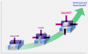
Evolution of Transistor Structure / Samsung
Samsung announced its GAA technology MBCFET in 2019 and released the first version of PDK. The GAA structure further mentions the contact area between the gate and the channel. It supports vertical stacking to obtain stronger current-carrying capacity, rather than stacking fins laterally like FinFETs. Samsung also announced that it will introduce GAA technology at the 3nm process node. According to the PPA data given by Samsung, the MBCFET of the advanced node has a 50% reduction in power consumption, a 30% increase in performance, and a 50% reduction in area compared with the 7nm FinFET.

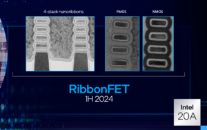
RibbonFET with stacked four layers of nanoribbons / Intel
The world’s first 2nm chip of IBM also uses nano-chip GAA technology. At the end of June 2021, Samsung announced that it has successfully taped out the 3nm GAA trial production chip cooperating with Synopsys. According to current news, Samsung is expected to launch 3GAE, an early GAA technology process in 2022, and 3GAP based on MBCFET in 2023. Intel also announced in the recent Intel Accelerated conference that it will introduce its GAA technology RibbonFET in its 20A process node, which is expected to be launched in the first half of 2024. And TSMC announced at this year’s technology forum that FinFET technology will only use 3nm, and 2nm will use nanosheet transistors to replace the existing structure.
However, what puzzles many people is that the names of the channels in GAA are nanowires, nanosheets, and nanoribbons. Are these different marketing terms or are there other secrets?
Nanowires, nanobelts and nanosheets
In fact, these are not fancy marketing terms, but different descriptions of the physical characteristics of the channel. The width of the nanowire and the thickness of the channel are basically similar. The nanosheet has a larger width. The nanobelt is a compromise solution, and it can also be regarded as a nanosheet with a smaller width. So how do different channels affect its performance? Due to the excellent short channel characteristics brought about by 2D structural constraints, nanowires perform better in low-power applications. And because of the larger effective width, the nanosheets achieve a larger contact area, and the current-carrying performance is better, which is suitable for some high-performance applications.

Cross-section comparison of nanowires and nanosheets / Samsung
Although the channels are different, Samsung and other manufacturers have adopted the method of stacking channels to continue to increase the current-carrying performance of the GAA structure. However, the fins in FinFETs cannot be superimposed infinitely, and the same is true for the channels in GAA. The improvement speed of this current-carrying capacity will be slowed down with the parasitic resistance at the source/drain epitaxy. Not only that, the gate capacitance will also increase with the increase of the number of channels, so in order to ensure the minimum RC delay , GAA generally chooses 3 or 4 channels.
2nm and the later transistor structure

Fork piece structure / IMEC
As for 2 nm and after transistor structure, the Belgian Microelectronics Research Center (IMEC) proposes a new alternative structure with a ForkSheet. In this configuration, the bifurcated gate structure controlle these nanosins. This structure introduces an insulating strength between PMOS and NMOS before gate patterning. It is opened by P-gate channel and N gate channel, providing NP pitch than the FinFET and nanoflakes. Thus, the fork sheet can provide better area and performance expansion capabilities. It can also reduce the cell height from 5T to 4.3T, and achieve a lower parasitic capacitance.

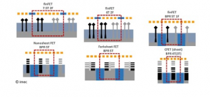
FinFET, nanochip, and CFET unit height contrast / IMEC
In order to advance the 1nm process, the cell height requirement has also been reduced to 3T. But due to the limitation of the distribution rate, even the bifurcated chip cannot meet this condition. Therefore, IMEC has introduced a technology called CFET, a complementary FET. The concept of CFET is to stack nFET on pFET, which provides more freedom for internal cell wiring and reduces cell area. In IMEC’s preliminary evaluation, the 4T FinFET using CFET technology can level or even exceed the standard 5T FinFET in terms of power consumption and performance, and occupy an area of 25% smaller. As for nanochip transistors using CFETs, not only can the logic cell height be 3T, but it can also provide additional performance improvements.
Conclusion
Just like the natural evolution of planar transistors to FinFETs, FinFETs will give way to GAAFETs. The process of structural evolution of CMOS devices is also a process in which semiconductors continue to challenge Moore’s Law. In addition, there are actually many companies that are exploring transistor solutions other than CMOS, trying to eliminate some of the shortcomings of CMOS itself, such as the Bizen launched by the British company Search For The Next. But judging from the current trend of pursuing PPA, these solutions are far from becoming mainstream in the market. In the semiconductor market after 2022, high-NA EUV lithography machines and GAAFETs will surely become key factors for processes below 5nm.


